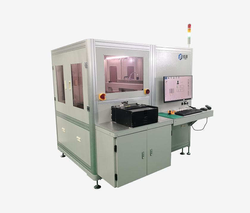
8-12Wafer inspection machine (after cutting)
main features
1. Suitable for optical detection after wafer cutting;
2. Non contact automatic AOI detection;
3. Compatible with SEMI standard 200-300mm Ring Wafer;
4. Compatible with SEMI standard baskets;
5. CMOS camera with a resolution of 7.3um/ pixe@0.75x ;
6. Field of view FOV15 * 15mm @ 0.75x, automatically adjustable magnification;
7. Support row/column/rectangular area inspection;
8. Support AOI detection for scratches, mold leaks, oil stains, stains, cracks, ink spots, and chipping edges;
9. Support SECS/GEM communication;
Equipment Usage
This device is an artificial microscope detection and judgment device used for the inspection of mounted wafers on 8 and 12 inch wafers (on membrane rings). Inspect the appearance quality of the chip after cutting the product.


