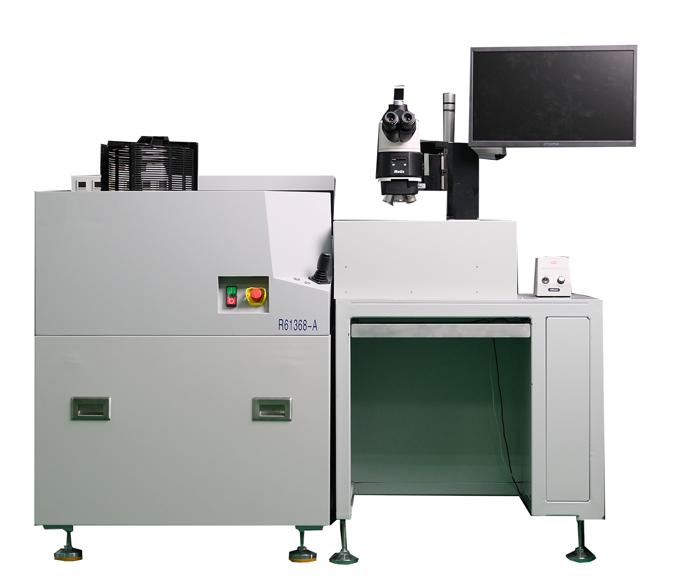
4-6 inch/6-8-inch wafer inspection machine
Main functions:
1. Suitable for optical detection before wafer cutting;
2. Automatic AOI detection, with no human contact throughout the process;
3. Compatible with SEMI standard 100-150mm (4-6 inches)/150-200mm (6-8 inches) Bare Wafer;
4. Compatible with SEMI standard H-Cassette;
5. Field of view FOV15 * 15mm @ 0.75x, automatically adjustable magnification;
6. Support row/column/rectangular area checking;
7. Support AOI detection for scratches, ink leaks, oil stains, dirt, cracks, ink spots, and chipping edges;
8. Support SECS/GEM communication;
9. Global wafer MAP/Review function;
10. The film transmission mechanism is modular and can be used independently;


